CMOS vs CCD
by Christian Buil

For spectrographic applications in particular, I compare the performance of Charge-Coupled Device (CCD) sensor with the latest generation of Complementary Metal Oxide Semiconductor (CMOS) sensors available to amateurs at the date (August 2017).
The focus is particularly on the Sony IMX290 CMOS detector and Panasonic MN34230PL detector that equips the ZWO cameras referenced ASI290MM and ASI1600MM. These detectors represents the state of the art, with performances close to the best scientific CMOS (sCMOS). In particular, the fact that the IMX290 readout noise (RON) is near 1 electron only give a real potential because this parameter is important in spectrography for detectivity. Also, this backside sensor type (i.e. electronic circuit not in the photo-sensitive side) display high quantum efficiency (QE), is attractive for faint detection applications.
The cameras concerned by this study are the ZW0 model ASI290MM-C00L, ASI1600MM-COOL (CMOS sensor) and the popular ATIK CCD cameras ATIK460EX and ATIK414EX. The detector chip (Panasonic origin) used in the AS1600MM cameras is the same one used in the Olympus OM-D E-M1 cameras (the monochrome version). See also ASI183MM Pro test page, a very new enlarged and performance improved version of ASI290MM-COOL camera.
PRIMARY OPTOECTRONIC PARAMETERS
The table below resume principal key optoelectronic features parameters measured by the author:

The electronic gain (in electrons/ADU) is computed by the relation:

where B is the mean value signal (in ADU) for a given area of a bias image, F is the mean value of the signal of the same area for a flat-field image (in ADU), σ(B1-B2) is the standard deviation of the pixels signal in the area of the difference of two bias images, σ(F1-F2) is the standard deviation of the pixels signal in the area of the différence of two flat field images.
The external camera (including detector) readout noise (RON) in electrons is given by:


The dark signal rate, in electrons/s/pixel, is given by:
where σADU is the standard deviation observed in the difference of two dark frame exposed each T seconds. The quantity measured is not strictly the pure thermal signal rate, but also a part of 1/f noise (see « Telegraph noise » section).
The given QE is relative to the estimated value for the Sony ICX694 detector (ATIK460EX camera). This latter sensor is therefore used as a reference (there is much confusion and imprecision in the literature about the quantum efficiency of the detectors, for example it is almost never specified whether if the QE includes the transmission of the protective glass - the values published are often imprecises and the origin of the results often unknown. For the ICX694 sensor, I adopted the values that seem the most reasonable for this component and consistent with what is published. The QE is given for a detector not equipped with its protective glass. To obtain the values with the protective glass, in all cases multiplied the QE results of the table by the coefficient 0.92 (transmission of a glass without anti-reflective coated).
The signal S for spectral QE evaluation is measured through a set of narrow interferential filters or at the focus of spectrographs (LHIRES III, ALPY600). The formulae used if the detector is 2D illuminated:

and for a binned spectral profile:

where S is the observed signal (in ADU), G is the electronic gain (in electron/ADU, in fact the reciprocal gain), P is the pixel size (in microns for example) and T is the integration time (in seconds for example) for the signal S.
The good news
The Read Out Noise (RON) of CMOS IMX290 is confirmed very small (1.1 e- at 20 dB gain setting). We are far then EMCCD but better then standard CCD. This value is impressive for a low-cost commercial device. In theory, if we consider a quantum efficiency of 70%, it is possible to detect potentially the arrival of only 7 photons in the integration time. We are not in photon counting regime, but not so far!
The RON is smaller (nearly 0.9 electron RMS) by setting the electronic gain to 40 dB (10 times the value of 20 dB gain), but the dynamic is too reduced for practical use of the detector.
Panasonic detector (ASI1600MM) is also very performant concerning the read out noise.
The IMX290 high quantum efficiency is a good new, superior to the excellent CCD ICX694 (note the 56% value at the blue level) - thanks to the Sony Exmor R back-illuminated technologie. The performance is reached with very small pixel (2.9 microns), impressive!
The readout speed of ASI290MM is also superior (full frame rate max. of 170 frame per second - USB3.0 recommended), 10 times the value of a classical CCD camera. The performance is of low interest for faint light spectroscopy (because we adopt here long integration time) but useful for autoguiding and instrumental ajustement.
The surface area of Panasonic chip is impressive for the cost. Excellent for capture for exemple the very full spectrum from UV to near-IR given by an Alpy600 spectrograph (Shelyak inst.) + the zero order image.
The bad news
The IMX290 Sony detector dark current rate is significantly superior to modern CCD for the same temperature (however, the the Panasonic sensor which equips the ASI1600MM appears more satisfactory on this point - see « dark current rate » section).
The thermal noise of the ASI290MM detector reach the value of the electronic read-out noise for an integration time of 20 seconds (at -22°C operating temperature). So, the thermal noise dominates for individual exposure greater then 20 seconds, which affect the excellent readout noise performance for long exposure.
The IMX290 and Panasonic chip colum-parallel A/D converter have only natively 12-bit resolution. The digital dynamic coding is inferior by a factor 16 relative to ATIK460EX. It is not a killer problem for faint spectrography, and if necessary, it is possible to segment in short exposure a long integration time.
CMOS doen't bin like CCDs .i.e. the Signal to Noise Ratio can’t improve by binning. I recommend always to use binning 1x1 mode with CMOS sensors - oversample by small pixels can be an advantage for reduce pseudo-noise, filtering of hot-pixels for example).
The presence of electroluminescent artifact and telegraphic non-gaussian noise is also evident on tested CMOS, see next sections…
DARK SIGNAL MAP
The ASI290MM images below is from a 300 seconds dark exposure at -22°C:
Left, the global aspect of dark signal. There is a noticeable electroluminescence produced by the electronic circuits of the sensor. The trace of this electroluminscence disappears completely in the science images when a correct map of dark reference is subtracted (same temperature and scaled intensity with respect to the exposure time). On the right, a detail of the dark image (or thermal signal). The structure is special, with some hot spots appearing blurry (diffusion ?), and others well like perfect points. Again, this structure disappears from the images science after a post-processing done according to the state of art. It is the most important.
Below the same for the ASI1600MM camera:

Electrolumiscence is also visible but with a significantly lower intensity (about 4x). The detailed aspect of the dark signal is closer to the standard encountered with the CCDs compared to the IMX290 detector situation.
DARK CURRENT RATE
The folowing table show the measured dark current in electrons/second/pixel for different functional detector temperatures:

The table show how the dark current is reduced by cooling the sensor. In all case, ASI1600MM Panasonic detector appear much better on this point then the ASI290MM Sony detector. Because a shot noise is associated with dark current, this status is of first importance when the issue is faint light detection with long time exposure. Per pixel and for the same temperature, the ASI1600MM thermal current rate is 10 times inferior compared to the ASI290MM.
ATIK460EX and ASI1600MM values (per pixel unit) are very similar, an excellent new concerning the recent CMOS technologie (but the pixel surface of Sony ICX694 is larger, so the dark current rate per pixel area unit is ultimately better for this component).
TELEGRAPH NOISE
Next figure, a high contrast display of successives offset images i.e. short exposure frames (here small part of 4 frames) show clearly presence of «random telegraph noise » (RTN), induced by impurity at pixel level (potential traps at the channel/oxide interface). About the telegraph noise manifestation: Some pixels appear to be animated by a random temporal blink over intensity. It is a low-frequency noise phenomenon in semiconductor devices, which is manifested as discrete random jumps in the drain current amplitude of CMOS transistors.


This 1/f noise character does not exist at this level with a CCD sensor. The noise of the CMOS tested is therefore not Gaussian. This means that there is a gain to average several elementary images to increase the Signal to Noise Ratio (SNR), the process is less effective compared to the result with a CCD detector.
LINEARITY
The response linearity is measured by observing the output signal (in ADU - Analog Digital Unit, or Digital Count) in function of integration time for a fix illumination of the detector. We compute also non-linearity error in percent i.e. the relative difference between observed signal and the better fitted linear function through the data.
Result for ASI290MM camera:

Result for ASI1600MM camera:

Result for ASI1600MM camera - detail of very faint signal dynamic region:

Comment. The linearity of the ASI290MM camera sensor is correct, but a transcription problem concerning the integration time command seem exist. Apparently, the jumps observed in the error function are related to a digital problem, either in the camera driver or in the sensor firmware. This means that the desired integration time is not exactly that achieved!
This digital control problem does not exist for the ASI1600MM camera, except perhaps for very short integration times (typically 0.005 sec). Over the vast majority of the Panasonic sensor dynamics, the linearity error is less than 1%, a remarkable performance. A larger error is detected between the floor signal level (98 ADU for my device, corresponding to a zero illumination) and an output signal of 102 ADU. That is to say that the nonlinearity exceeds 1% for only the first 4 LSB of the dynamics, which is almost imperceptible in practice.
The CMOS cameras tested are capable of high quality photometric measurements without requiring external correction of nonlinearity.
The Panasonic sensor that equips the ASI1600MM camera reveals it as an excellent measuring tool for scientific work.
FRINGES
One of the most critical problems posed by the cameras used for spectrography is the generation of fringes patterns. These fringes are created by the interference of quasi monochromatic light within protective parallel glass plates. In presence of fringe phenomena, the intensity of the spectral continuum can sometimes be significantly modulated. When the problem exists, and if it is not properly corrected, the radiometric quality of the acquired data is degraded and prevents serious scientific exploitation.
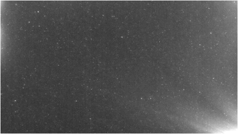
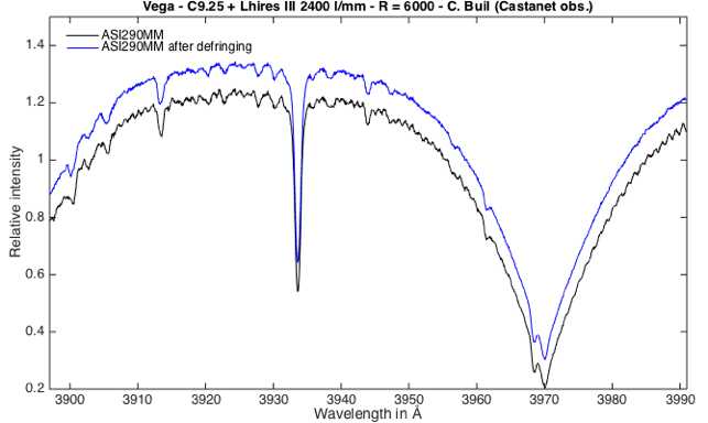
The ASI290MM camera attached to a LHIRES III spectrograph (for medium and high resolution spectrography) unfortunately deliver a very marked fringes phenomenon (also the ASI1600MM and ATIK414EX, see below).
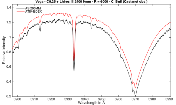
Here an example for the blue part of Vega star spectrum, in the vicinity of Ca II H & K lines. We compare here a spectrum of the same object taken with an ATIK460EX camera (red line) and an ASI290MM camera (black line). The continuum modulation presence is clearly detected in the spectrum made with this last camera.
A rigorous procedure is necessary during the data acquisition and during post processing phase in order to eliminate the pseudo noise induced by the fringes (if no, the fringes pattern is a detector killer). Here the ASI290MM spectrum rectified for remove the fringing effect (« defringing » operation):
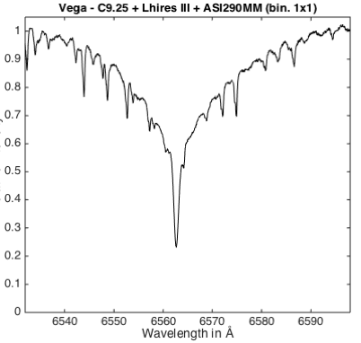
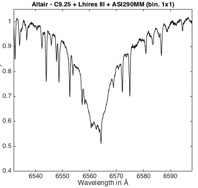
Another dramatic illustrations of the fringes observed with the ASI290MM camera, for this time the red region of the spectrum, around the Halpha line, left for Vega star, right for Altair star:
Of course, the ASI290MM camera is not the only one that generates fringes in spectrography! As an exemple, the following tests concern the measurement of spectral transmission of the ASTRODON Halpha 6-nm filter located just in front of the LHIRES III spectrograph entrance slit (2400 line / mm):
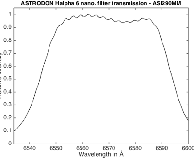
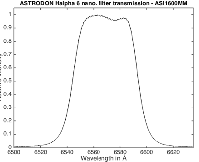
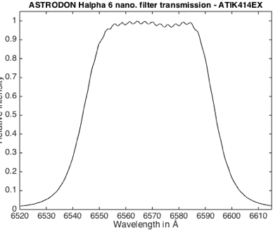
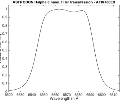
All the cameras tested here (ASI290MM, ASI1600, ATIK414EX) show fringes ... except the ATIK460EX model, and also the very new and excellent ASI183MM camera (Sony IMX183 backside CMOS - see here the dedicated evaluation page).
At the wavelength of λ=6563 A, the measured pitch of the fringes for the ASI290MM camera is Δλ=2.88 A. It is deduced from this result and the formulae,

that the thickness of responsible cavity is e=0.5 mm (for a refractive index of n=1.5). The camera's input protective plate can not be responsible because it is 3 mm thick piece on this model and surfaces are covered by a very effective anti-reflective coating. The silicon structure of the detector is also excluded because the pitch of the fringes pattern is too small and too regular. Finally, the optical element at the origin of the fringes can only be the cover glass of the detector itself (the calculated thickness is coherent).
The situation of the ATIK460EX camera is particular (and welcome!). By a simple visual inspection, the light intensity reflected by the detector glass protection reveals at least twice (but surely more) less intense than that reflected by the cover glass of other models (ASI290, ATIK414EX ...). This visual effect is striking and indicates that the Sony ICX694 cover glass has a special anti-reflective coating, while the reflection coefficient for the other sensor is about 0.92 per side. This is most probably the origin of the absence of fringes in the case of the ATIK460EX camera.
Fringes are difficult to remove without significant effort during acquisition and possible manual adjustment during processing, which is a time-consuming exercise, but necessary for reliable science (note: the actual fringes problem only concerns spectrographs which can reach resolution power greater than 2000. For inferior resolution - the situation of Alpy600 or LISA spectrographs for example - the fringes are not resolved. Also, it is worth remembering that all reduction steps add noise to the image…
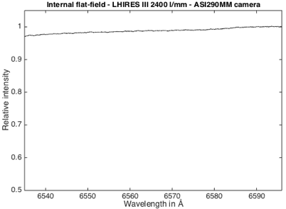
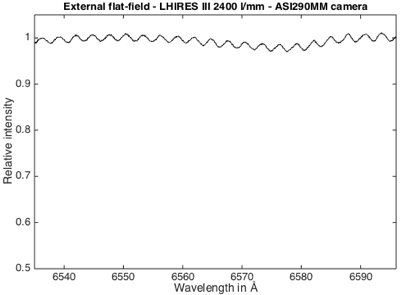
How to remove the fringes ? First, I realize a flat-field with a very high signal to noise ratio - see right image.
The internal tungsten lamp system of the LHIRES III spectrograph is deficient for this operation. This is an important point to note and a critical problem to consider. The reason is simple: The slit cavity of the LHIRES III leaves a wide free passage to the light of the lamp outside the narrow slit:


The flat-field thus obtained has nothing in common with that necessary to correct the data in almost all situations (dust, vignetting, ...). The fringes are not visible because the detector is mostly illuminated by a polychromatic light! The internal flat-field source of the LHIRES III is no operand. Dommage ! An alternative solution consist to use a (robust) front flit-mirror system for inject a white light flux for flat-field operation (and also spectral calibration lamp light for a maximal precision).
I recommande also to insert a 5 mm diaphragm at some distance front of the slit for limit parasitic light entrance - see at right.
Proof of « external » flat-field efficiency compared to « internal » flat-field for extract fringes pattern - below fringes are virtually invisible in the internal lamp flat-field profile:

For the correction, the object profile is divided by the (external) flat-field profile extracted from the same area of the sensor, carefully spectrally calibrated and slightly scaled if necessary (contrast adjustment). The example for Altair spectrum:


PIXEL RESPONSE NON UNIFORMITY (PRNU)
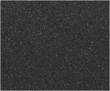
The right image from ASI290MM is an enlargement (4x) of a small portion of a detector flat-field image. It is a very high contrast display in order to identify small pixel response differences while the detector is illuminated by a uniform source (PRNU map is obtained with a high signal-to-noise ratio in order to make the noise negligible).
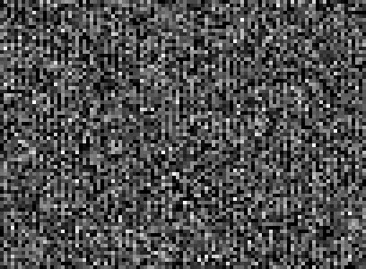
The RMS gain variation between pixels is near 0.7% for the ASI290MM detector. A very slight vertical pattern can be identified (probably because Exmor has internal column A/D converter). This is a very good result for CMOS technology (remember, here each pixel is drived by an individual « amplifier »). The statistical PRNU fluctuation of IMX694 CCD sensor is measured to 0,3%.
How to extract a PRNU reference map ? (1) The detector surface is illuminated approximately uniformly (by using this time the internal flat-field lamp of the LHIRES III spectrograph, this time useful), (2) The high frequency component of the flat-field image is extracted by using a specific tools of ISIS software (MASTERS tab):

ON THE SKY
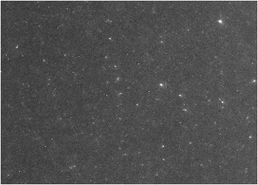
HD 217813 is an exemple of chromospheric active star. The activity (equivalent to faculae plage and protuberances for the Sun) can be detected by observing the core of Ca II H & K lines in the near ultraviolet. The magnitude is 7.3 at the level of H&K lines. The object is observed by using a C9.25 telescope (D=23.5 cm) and a Lhires III spectrograph. The latest is equipped by a 2400 l/mm grating and a 35 microns wide entrance slit. The spectral resolution power is R=6000.
The target is observed with the same setup but by using a ATIK414EX CCD camera and a ASI290MM camera respectively. Here the result:
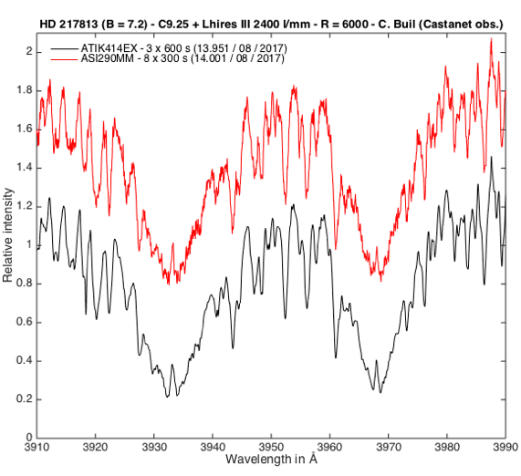
First, the chromospheric emission is detected: the emission peak at the level of H&K lines. Secondly, this detection is within the scope of a CMOS camera, here the ASI290MM. This is a true indication of the progress made by CMOS detectors!
At the present time, ASI290MM spectral profile is more noisy then ATIK460EX profile. The principal reason are, (1)
a spectral sampling not adapted to the characteristics of the spectrograph used (the spectrum is largely oversampled), (2) a too high dark signal (thermal noise) which destroys the benefit of very low reading noise.
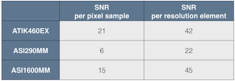
The table below resume the calculated SNR (Signal to Noise Ratio) on this star, for the H&K region, for an integration time of one hour (stack of 6x600 sec. exposure), and for the ATIK460EX, ASI290MM and ASI1600MM camera (the used instrumental simulator tool is from the author):
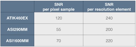
The important performance indicator is the « SNR per resolution element ». The ATIK460EX is the better device (highest signal to noise ratio), but CMOS are not so far. The ASI1600MM camera appears to be more performant compared to the ASI290MM camera in this simulation because inferior thermal noise, although the RON is slightly higher and the quantum efficiency is lower (see table above this page). The large sensitive surface of ASI2600MM detector can be also an advantage (important when using LISA ou ALPY600 spectrograph, for exemple).
To show the situation more better, the next table present the relative distribution importance of elementary noises source that contribute to the final SNR performance (for one-hour observation of HD 217813):

For the ATIK460EX, the photon noise of the object dominate, in second the readout noise. For the ASI290MM (and also ASI1600MM), the principal noise contributor is the object photon noise, and the second the thermal noise. It’s a key difference between CCD and CMOS camera at the present time. The ATIK460EX is used at -10°C, the ASI290MM at -22°C, the ASI1600MM at -20°C. For given an idea, the ASI290MM camera must be operated at temperature of approximatively -45°C to match the thermal signal of ATIK460EX at -10°C.
The noise from the sky background is insignificant for all situation. It is a feature of long slit spectroscopy. It is another story for deep sky observation…
The next table give the status for ultra faint object spectroscopy: Observation of H&K lines with a C9.25 and Lhires III at R=6000, but for a magnitude 10 star:
The performances of ATIK46EX and ASI1600MM cameras are now really equivalent. The ASI290MM camera is clearly inferior because the relative thermal noise appears dramatically high (65% of the total):

In the other hand, a camera equipped with the Panasonic MN34230PL detector operated at a temperature of -30°C would make this detector a very concurrent choice to the CCD for ultra faint flux observation and long time exposure observational mode - thanks to the excellent reading noise performance of this CMOS sensor. Because it’s vast sensitive surface, it could be for example a fine solution for an echelle spectrograph.
The CMOS sensors are making continuous progress and some camera manufacturers will surely have the idea to cool the sensor much more. A revolution is in progress! Presently, low cost CMOS cameras are a credible choice for the discovery of spectrography, and also for make some real science…