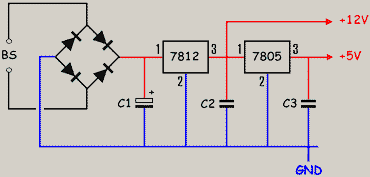
Digital electronics requires mostly 2 ranges of voltage.
TTL Circuits must be fed with 5 volts and CMOS circuits require
a 3 to 18 volts and are generally fed in 12 volts. Other elements
use frequently these voltages: fans, motors, relays, etc....
The simplest consists in using an adaptor. It delivers generally
some hundreds of mA and 15 - 25 V but without stabilization.
The use of a bridge rectifier allows to be quiet with the polarité of
the connector. The integrated regulators are very easy to use.
It could be necessary to equip them with a heat-sink.
|
Pin Assignments for
LM7805 and 7812
- V in
- Ground
- V out
|
|
Components List
Bridge rectifier or 4 diodes 1N4002
Capacitors : C1 = 1000 µF 25 V
C2, C3 = 220 nF
regulators : LM 7812, LM 7805
Adaptor (BS) 500 mA |
|
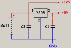
In the case of a 12 volts battery as electric power supply (we can intend to go to fields with his spectroheliograph), the plan is reduced to the production of a tension regulated to 5 volts.
|
| |
|
Components List
see previous
12 Volts battery
|
|
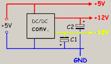
The use of operational amplifiers also requires the production of negative voltages. Various assemblies are still possible, the simplest being the use of an integrated converter. We can then, from a 5 volts supply, get symmetric voltages 12 and -12 volts.
|
| |
|
Components List
Capacitors : C1,C2 = 220µF 25 V
5V regulated power supply
DC/DC converter : PM951
|
|
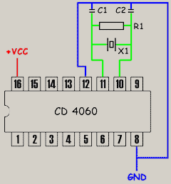
Clock pulse generator / binary counter
This digital circuit (CD 4060) allows to produce a stable square signal of high frequency by means of a quartz and very few secondary components. Its counter function (divide by 2 counter) allows to find one frequencies suited for the clocks of the CCD.
|
|
Pin Assignments for CD4060
- Q12
- Q13
- Q14
- Q6
- Q5
- Q7
- Q4
- Ground
- clk2
- clk 1
- clk
- reset
- Q9
- Q8
- Q10
- +Vcc
|
|
Components List
Resistor : R1 = 10 MΩ
Capacitors : C1, C2 = 4.7 pF
Quartz : X1 = 12 MHz
digital circuit : CD 4060
Power supply VCC : 5 to 18 V |
|
Output Qi delivers a frequency equal to the quartz frequency divided by 2 at the power i (ex: Q5 gives Freq / 32)
|
|
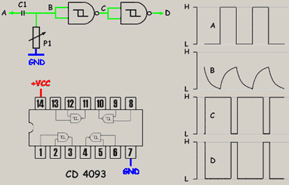
Changing the pulse width
The previous assembly gives a rectangular
signal with a duty cyclic equal to 50
%. We can need to change it
to produce pulses for example. A simple means is to use
a variable RC circuit and to reshape the signal obtained
by means of a Schmidt trigger , here a CD 4093 which
allows to use a wide range of voltage. (The CD 4093 is in
fact a quadruple logic gates NAND which we use here only
the inverter function).
|
|
Pin Assignments for CD4093
- In1
- In1'
- Out1
- Out2
- In2
- In2'
- Ground
- In3
- In3'
- Out3
- 1Out4
- In4
- In4'
- +Vcc
|
|
Components List
Pot. : P1
= 20 kΩ
Capacitors : C1, 33 pF
digital circuit : CD 4093
Power supply VCC : 5 to 18 V |
|
Modifying the value of P1 we make vary the height
of the signal (B) which is not any more squarewave but sawtooth.
The trigger activates when a threshold is reached
and we so obtain a modified duty cycle (C and D). |
|
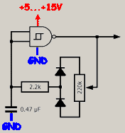
PWM generator (pulse width modulation)
Here is an assembly very simple
to get an oscillator giving a fixed frequency signal but
variable duty cycle. It can - after amplifier transistor
- serve to control the rotation speed of a motor with direct
current or to adjust the power of a dew-heater.
We use once again a logic gate of a CD4093 circuit.
|
|
Pin Assignments for CD4093
- In1
- In1'
- Out1
- Out2
- In2
- In2'
- Ground
- In3
- In3'
- Out3
- Out4
- In4
- In4'
- +Vcc
|
|
Components List
Pot. : P1 = 220 kΩ
Capacitors : C1, 0.47 µF
diodes 1N 4148
resistor 2.2 kΩ
digital circuit : CD 4093
Power supply VCC : 5 à 15 V |
The frequency of oscillations is easily modifiable by changing the value of the capacitior. The unused pins of the CD4093 must be connected to ground. |
|
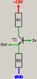
Amplification of video
The video signal going out of the
CCD is low level and it is necessary to amplify it to allow
a good transmission in a long cable.
|
| |
|
Components List
Resistors :
R1 = 100 Ω, R2 = 1 KΩ
Transistor : T1 = 2N2222
|
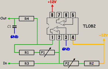
| The voltage of the
video signal varies the other way of the illumination.
It is thus necessary to invert this signal and to move
its origin so that the voltage is equal to 0 for
a no illumination and so that it increases when the illumination
increases. The operational amplifiers are the ideal solution
for this work.
|
|
Pin Assignments for TL082
- out 1
- inv inp 1
- non-inv inp 1
- -Vcc
- non-inv inp 2
- inv inp 2
- out 2
- +Vcc
Il y a donc 2 amplis-op dans ce boitier. |
|
Components List
Resistors : R1 = 1 kΩ, R2,R3 = 2,2
kΩ,
R4 = 470 Ω
Pot. : P1,P2 = 10 kΩ
Capacitors : C1 = 10 nF
Op-Amplifier : TL 082 |
|
circuit R4,C1 circuit is a filter able to limit high frequencies.
|
|
Analogic / Digital converter
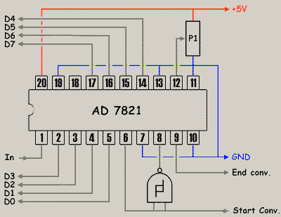
This integrated circuit (AD 7821) allows to convert an analogic signal in a 8 bits value with a 1 µs conversion time, thus with a 1 MHz frequency. There are faster converters allowing to obtain a better resolution (10, 12, 14 or 16 bits).
|
|
Pin Assignments for AD7821
- Input
- Data bit 3
- Data bit 2
- Data bit 1
- Data bit 0
- WR/RDY
- Mode
- RD
- INT
- Ground
- Vref -
- Vref +
- CS
- Data bit 4
- Data bit 5
- Data bit 6
- Data bit 7
- OFL
- Vss
- +Vcc
|
|
Components List
Pot. : P1 = 20 kΩ
A/D Converter = AD7821
trigger inverter = 1/4 CD4093 |
|
The signal resulting from the amplifier is applied to the pin 1 (Input). The reference voltage is adjusted by means of P1. It is very summary but that works. We can also use a specific component to obtain this reference voltage (zener diode for ex.).
The pulse "start of conversion" results from the clock generator (having a 5 V level compatible with the converter) and the pulse "End of conversion" is sent to the PC interface, as well as 8 bits data. We can also send these data through buffer circuits (74245 by eg) to secure the exchanges interface-converter. The logic gate (1/4 CD4093) can be another inverter.
|
|
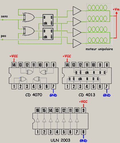
Stepper motor drive
Integrated circuits intended to drive stepper motors
are many and are rather easy to operate because they contain
both logical circuits and power circuits
in the same chip. You just have to choose the circuit corresponding
to the type of stepper motor you want to use,
namely unipolar (6 wires) or bipolar (4 wires).
In the first case, we can use a SAA on 1027 (difficult to find now) or a more powerful UCN 5804. For the bipolar motor, the SAA 1042 (idem) or the MC 3479 will be quite indicated. Most of these controllers allow to work in half-step mode.
It is to note also that we can drive a unipolar motor with a controleur for bipolar motor but that the opposite is not possible.
We propose here a plan of driver for unipolar motor realized with 2 common logic components and a power circuit. It is possible to drive motor needing 500 mA by coil, what should be sufficient in the present frame! |
|
Pin Assignments for CD4070
- In 1
- In 1'
- Out 1
- Out 2
- In 2
- In 2'
- Ground
- In 3
- In 3'
- Out 3
- Out 4
- In 4
- In 4'
- +Vcc
Pin Assignments for CD4013
- Out 1
- Out inv 1
- Clock 1
- Reset 1
- Data 1
- Set 1
- Ground
- Set 2
- Data 2
- Reset 2
- Clock 2
- Out inv 2
- Out 2
- +Vcc
|
|
Pin Assignments for CD4093
- In 1
- In 2
- In 3
- In 4
- In 5
- In 6
- In 7
- Ground
- +Vcc
- Out 7
- Out 6
- Out 5
- Out 4
- Out 3
- Out 2
- Out 1
Components list
IC :
quad. XOR = CD 4070 or 4030
Dual shift register = CD 4013
Ampli = ULN 2003
Unipolar stepper motor
|
|
Stepper motors can be found on old floppy disk drives or printers for example. In certain cases we can even use the controllers who are joined to it. 2 control pulses can result from a microcomputer (parallel port) + line buffers.
Other intergated circuits
|
|
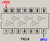
Pin Assignments for 7414
- In 1
- Out 1
- In 2
- Out 2
- In 3
- Out 3
- Ground
- Out 4
- In 4
- Out 5
- In 5
- Out 6
- In 6
- +Vcc
|
|
Hex trigger inverter
(TTL)
|
|
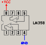
Pin Assignments for LM358
- out 1
- inv inp 1
- non-inv inp 1
- GND
- non-inv inp 2
- inv inp 2
- out 2
- +Vcc
|
|
dual monotension opAmpli : LM358
+VCC from 5 to 15V |
| |

 )
)